Nowadays, the employment of solar power plants is usual across the world. We know, the main source to produce solar energy is the source of sunlight. Solar energy is growing popular for generating power, heating, and chlorinating water all around the world.
The sun initiates nuclear reactions, which results in the production of solar energy. When protons from hydrogen atoms hit forcefully in the center of the sun, they react to form a helium atom. The solar energy that reaches Earth is allow to reflect back into space to the tune of 30%. The earth covers the remaining energy. The radiation heats the Earth’s surface, which then radiates some of the energy back out as infrared waves.
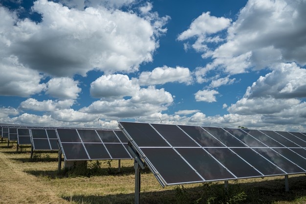
The production process of solar power plant
There are series of processes that are present in the production of solar energy panels. Photovoltaic (PV) systems account for the majority of solar manufacturing in the United States. PV modules, cabling and wiring, power converter, and system monitoring equipment are all made in the United States.
Raw material
The most crucial or basic element for making solar energy panels is pure silicon. The absorber material in most commercially available PV modules is crystalline silicon.
Production steps
There are various manufacturing phases in the production of these modules, which usually take place in the sequence.
From raw quartz to solar cells, a series of stages are necessary, beginning with the separation and purification of silicon. It is then chopping it into usable discs – silicon wafers – that are further processing into ready-to-assemble solar cells.
Step#1: manufacturing of silicon wafers
The impure silicon dioxide in quartz is first ground and then purify to get pure silicon, which is usable for the production of silicon wafers. The first stage involves placing powdered quartz in a special furnace and using a carbon electrode to produce a high electric arc between the electrode and the silicon dioxide. The pure silicon is now ready for further process.
Step#2: doping process
To make a semiconductor capable of carrying electricity, the resulting pure silicon is doping (processed) with phosphorous and boron to produce an excess of electrons and a shortage of electrons, respectively. The process of doping is the addition of contaminants to a crystalline silicon wafer in order to make it electrically conductive.
Step#3: generating solar cells from silicon wafers
The main and most vital step in the production of solar cells from silicon wafers. This is the large step comprising of 9 sub-steps.
- Pre-treatment: The raw silicon wafer discs are inspected for damages such as fractures, breakages, scratches, and other irregularities during the pre-check process.
- Texturing: After the initial pre-check, the front surface of the silicon wafers is textured to reduce incoming light reflection losses.
- Acid cleaning: After the process of texturing, the wafers are rinsed in an acidic solution. Any post-texturing particle residue is take out from the surface in this stage. Chloride particles absorb metallic residue on the surface, using hydrogen chloride acid (HCl).
- Diffusion: Diffusion is the technique of making a silicon wafer more electrically conductive through adding dopants to it. Solid-state diffusion and emitter diffusion are the two most common types of diffusion. Wafers pre-doped with p-type boron during the casting process acquire a negative (n-type) surface during the process of diffusion when diffusing them with a phosphorous source at high temperatures, results in the positive-negative (p-n) junction.
Step4: Etching or cleaning
- Etching process: Firstly disc stacking the cells on top of each other and then subjecting them to a plasma etching chamber using tetrafluoromethane (CF4) to etch exposed edges, the etching and edge isolation procedure removes the electrical channel around the wafer edge.
- Post etching process: Particle deposits on the wafer and the wafer edges may remain after etching. As a result, the wafers undergo washing again to remove the traces of the prior etching procedure.
- Anti-reflective coating deposition: AR coating is frequently added to the surface in addition to surface texturing to reduce reflection and increase the quantity of light absorbed into the cell. Because the reflection of naked silicon solar cells is about 30%, this anti-reflective coating is critical. Silicon nitride (Si3N4) or titanium oxide (TiO2) are active for the thin AR Coating. This procedure uses a high power to knock particles off the substance and deposit them on the silicon at the respective electrodes. Allowing silicon to react with oxygen or nitrogen-containing gases to form silicon dioxide or silicon nitride is another method. Silicon nitride is useful in commercial solar cells.
Step#5: Finishing
- Printing and dyeing: Metal inlines are put to bed on the wafer next, with the goal of creating ohmic connections. Backside printing is the process of printing metal shaped on the back of a wafer.
Using specific screen printing techniques enables to insert of metal inlines on the backside of the metal pastes. The wafer undergoes drying when it is fabricate. .
The screen-imprint wafers are then transmitting through a sintering furnace to cement the dry metal pastes onto the wafers once all contacts are allow to process on the back and front sides. After that, the wafers are allowing to cool and are ready to process as solar cells.
- Testing and cell sorting: The now-ready-to-assemble solar cells are evaluated under simulated sunshine conditions and then categorized and sorted based on their efficiencies in this final step.
A solar cell testing gadget takes care of this, testing and sorting the cells automatically. The production workers must then simply remove the cells from the efficiency repository into which the machine had sorted them. After that, the solar cell essentially becomes a new raw material that is active in the construction of solar PV modules. The final result in the form of a solar cell is then further classify into multiple solar cell quality categories based on the smoothness of the production process and the basic silicon wafer material quality.
Conclusion
In this context, the main theme of this article is to provide information to people or users about the production of solar energy or cell, passing different steps or stages.
Developing and producing less-priced alternatives to crystalline silicon cells is one example of Solar Power Equipments innovation. Solar windows that simulate photosynthesis and smaller cells constructed from amorphous silicon balls are two of the options. Amorphous and polycrystalline silicon are already outperforming single crystal silicon in terms of attractiveness. Other innovations include employing prismatic lenses to focus sunlight and reducing shadow.